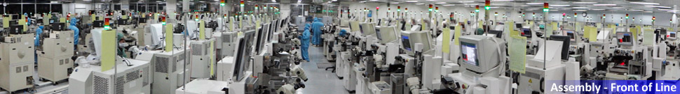
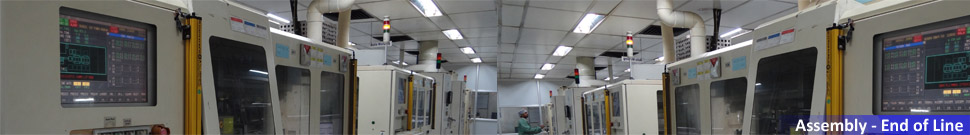
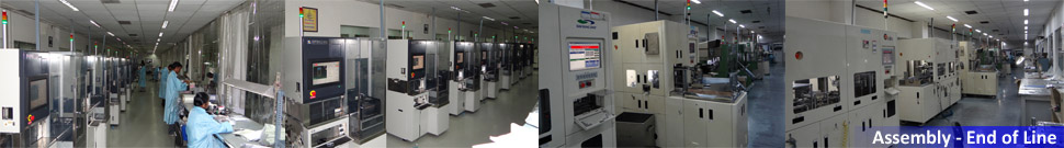
Position: BGA Packaging Engineer

Designing single die, multi die BGA, Chip Scale laminate BGA, review and optimize new substrate according to design spec for new packages (feasibility, trace routing, design spec., etc)
Perform electrical and package simulation in relation to substrate design and data analysis (inductance, resistance, voltage, power etc) and be able to identify the root cause for substrate related issue.
Deal with substrate supplier in qualifying new substrate technology or roadmap
Work closely with the process team to further improve process stability
Responsible for New Package Qualification project leader to coordinate the progress of all engineering and qualification lots. It also include coordinating the progress of FAI, reliability test and BOM generation and documentation
Responsible for Material engineering integration to support material related issues and challenges, value engineering activities (i.e. cost saving) and design for manufacturability in new packages

Requirements

Please eMail your resume to hr@natronix.net


News & Events


© 2011 Natronix Semiconductor Technology Limited. All Rights Reserved.  
Designed & Developed by Cherrytec