Defining The Future Through Partnerships

Natronix Semiconductor Technology 

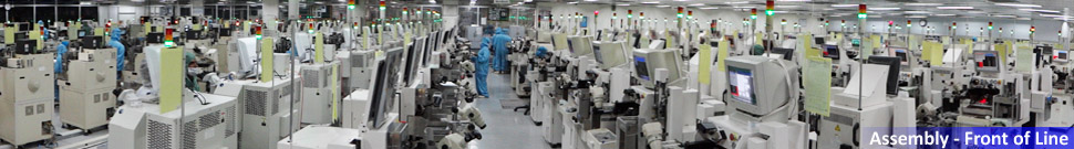
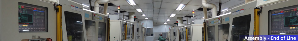
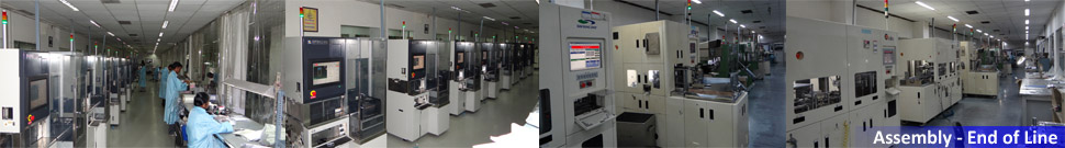
an OSAT & Design Company-


SPEL’s Packaging Portfolio broadly classified into Leaded (Through hole & SMD)  packages and QFN packages. Offers one of Industry’s widest range of packages in QFN with the footprint options from 0.5mm2 to 12.0mm2 and thickness options from 0.4mm to 0.9mm.

 
  SPEL’s QFN / DFN package have the following advantages
   
 
  • QFN wettable flank Packaging options
   
 
  • Wide range of Packages already tooled up for immediate Customer Qualification
   
 
  • New Package can be developed in 4weeks time & at very low Cost using its in-house Design expertise
   
 
  • Jedec and non Jedec Custom Package options
   
 
  • Use of Assembly & Process Technologies like Chip on Board (COB) and Wafer Backside Coating for reduced package foot-print
   
 
  • Multi Die, Multi Wire, Stacked Die capability
   
 
  • Wire-Bonding options – Au Wire, Cu Wire, PdCu Wire
   
 
  • Lead-Finish option – 100% Sn, NiPdAu
   
 
  • Shipment options – Tray, Shipping Tube, Cannister
   
 
  • Complementing Test Toolings for Cost effective Turnkey Solution
 

SPEL’s Package Road Map is aligned with evolving Industry and Customer requirements reinforcing the commitment of providing Cost effective & high Quality packaging solutions.


SPEL Semiconductor Limited is India’s first & only Semiconductor IC Assembly & Test facility. SPEL pioneered the Outsourced Semiconductor Assembly & Test Services (OSAT) market in India and continues to steadily do so. SPEL is a trusted & strategic contract manufacturing partner for many of the world's leading Semiconductor companies.

SPEL Center Page


Copyright © 2023 Natronix Semiconductor Technology Pte Ltd. All Rights Reserved.

Best viewed at 1366 x 768 resolution in IE11 & Safari v5